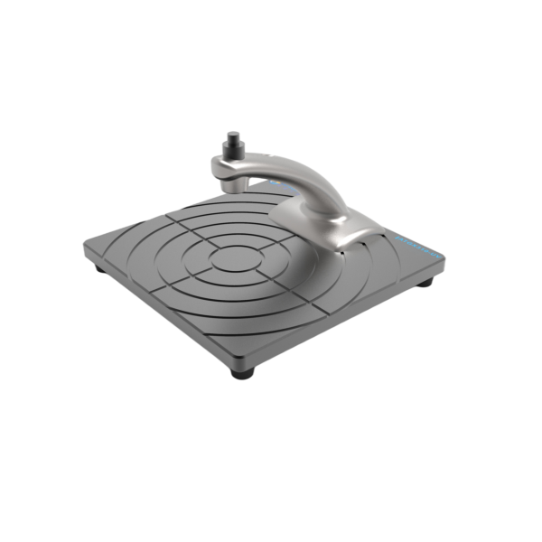
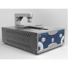
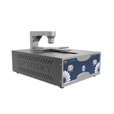
SM200 is an automatic thin film thickness mapper developed by utilizing the principle of thin film reflected light interference. It uses the light with the widest wavelength range of 200-1700nm to vertically incident on the surface of the thin film. As long as the thin film has a certain degree of transmission, the SM200 can calculate the thickness of the film according to the reflected interference spectrum, as well as other optical constants such as reflectivity. , refractive index and extinction coefficient, etc., the thickness of the maximum mapping range can reach 1nm ~ 250um.
The SM200 automatic optical thin film thickness mapper is constructed by the surveying and mapping host, the surveying and mapping platform, the Y-type optical fiber and the host computer software. The leading generation of automated optical film thickness gauges.


- Semiconductor coating: photoresist, oxide, desalination layer, silicon-on-insulator, wafer back grinding;
- Liquid crystal display: gap thickness, polyimide, ITO transparent conductive film;
- Optical coating: hard coating, anti-reflection layer;
- Microelectronic system: photoresist, silicon film, printed circuit board;
- Biomedical: medical equipment, Parylene
SM200 Optical Film Thickness Gauge | ||||
Model | SM200-LUV | SM200-HUV | SM200 | SM200-NIR |
General specifications | ||||
Spectral range | 200nm-1000nm | 200nm-1000nm | 400nm-1000nm | 900nm-1700nm |
Light source | Deuterium halogen Lamp | Tungsten halogen lamp | ||
Measurement specifications | ||||
Thickness range1 | 1nm-10um | 1nm~30um | 20nm-60um | 100nm-250um |
Accuracy2 | ±2nm或0.2% | ±3nm或0.4% | ||
Incidence angle | 90° | |||
Film thickness layers | 1~3 | |||
Sample material | Transparent or translucent film | |||
Measurement mode | Single-point/multi-point/automated measurements | |||
Spot size3 | 2mm | |||
Sample size | Diameters from 1mm to 300mm or larger | |||
Basic requirements | ||||
Operating system | Windows10/11 | |||
Indicator light | Deuterium lamp indication, halogen lamp indication | Halogen lamp indication | ||
Button | Power buttons, deuterium lamps, halogen lamps | Power button, halogen power | ||
External interface | Power outlet, USB 2.0, RJ45 | |||
Scanning platform | Rotate + X axis movement | |||
Movable stroke | 150mm*360° | |||
Material | Aluminum alloy | |||
Power supply | 100~240VAC,50~60Hz | |||
Packing list | Mainframe, measuring platform, power cord, communication cable, optical probe, Y-fiber | |||
Remarks: 1. Depends on the material; 2. The larger one is the larger and depends on the material; 3. Optional up to 20um; | ||||


