Your shopping cart is empty!
film thickness tester


Availability: In Stock
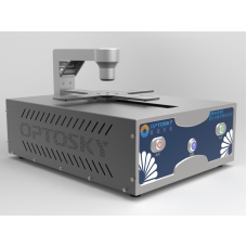
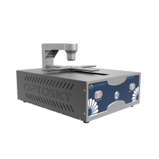
film thickness tester
Product Code: SM230
application
SM230 is an automatic thin film thickness mapper developed by utilizing the principle of thin film reflected light interference. It uses the light with the widest wavelength range of 200-1700nm to vertically incident on the surface of the thin film. As long as the film has a certain degree of transmission, the SM230 can calculate the thickness of the thin film according to the reflected interference spectrum, as well as other optical constants such as reflectivity, refractive index and extinction coefficient, etc., the thickness of the maximum mapping range can reach 5nm ~ 250um.
The SM230 automatic optical thin film thickness mapping instrument is constructed by the surveying and mapping host, the surveying and mapping platform, the Y-type optical fiber and the host computer software. technology, providing users with a new generation of leading automatic optical film thickness mappers.


- Non-contact, non-destructive testing system;
- Ultra-long life light source, higher luminous efficiency;
- High-resolution, high-sensitivity spectrometer, more accurate and reliable mapping results;
- The software interface is intuitive, and the operation is convenient and time-saving;
- The surveying and mapping speed is fast, and it supports multi-point surveying and mapping point map drawing;
- Support drawing 2D/3D thickness distribution map of samples;
- High-precision, long-life 3-axis rotary platform;
- Historical data storage to help users better grasp the results;
- Desktop distribution design, suitable for rich scenarios;
- Low maintenance cost and convenient maintenance;
- Biomedical: medical equipment, Parylene
- Optical coating: hard coating, anti-reflection layer;
- Semiconductor coating: photoresist, oxide, desalination layer, silicon-on-insulator, wafer back grinding;
- Microelectronic system: photoresist, silicon film, printed circuit board;
- Liquid crystal display: gap thickness, polyimide, ITO transparent conductive film;
SM230 Automatic Optical Film Thickness Mapper | ||||
Model | SM230-LUV | SM230-HUV | SM230 | SM230-NIR |
General specifications | ||||
Spectral range | 200nm-1000nm | 200nm-1000nm | 400nm-1000nm | 900nm-1700nm |
Light source | Deuterium halogen Lamp | Tungsten halogen lamp | ||
Measurement specifications | ||||
Thickness range1 | 5nm-10um | 5nm~30um | 20nm-60um | 100nm-250um |
Accuracy2 | ±2nm或0.2% | ±3nm或0.4% | ||
Incidence angle | 90° | |||
Film thickness layers | 1~3 | |||
Sample material | Transparent or translucent film | |||
Measurement mode | Single-point/multi-point/automated measurements | |||
Spot size3 | 2mm | |||
Sample size | Diameters from 1mm to 300mm or larger | |||
Basic requirements | ||||
Operating system | Windows10/11 | |||
Indicator light | Deuterium lamp indication, halogen lamp indication | Halogen lamp indication | ||
Button | Power buttons, deuterium lamps, halogen lamps | Power button, halogen power | ||
External interface | Power outlet, USB 2.0, RJ45 | |||
Scanning platform | Rotate + X axis movement | |||
Movable stroke | 150mm*360° | |||
Material | Aluminum alloy | |||
Power supply | 100~240VAC,50~60Hz | |||
Packing list | Mainframe, measuring platform, power cord, communication cable, optical probe, Y-fiber | |||
Remarks: 1. Depends on the material; 2. The larger one is the larger and depends on the material; 3. Optional up to 20um; | ||||