Your shopping cart is empty!
reflected light


Availability: In Stock
reflected light
Download Data Sheet
Product Code: SM280
application
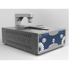
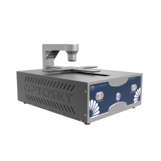
SM280 is a microscopic thin flim thickness measuring instrument developed by using the principle of thin film reflected light interference. It uses the light with the widest wavelength range of 200-1700nm to be vertically incident on the surface of the film. As long as the film has a certain degree of transmission, the SM280 can calculate the film thickness according to the reflected interference spectrum. The thickness of the maximum mapping range can reach 10nm ~ 100um. SM280 is equipped with a dedicated microscope system, which can support the test of tiny samples with a minimum size of 10um. The software has template matching and auto-focus functions, and supports the drawing of measurement point paths and presentation of measurement results in 2D/3D.
SM280 automatic microscopic film thickness measuring instrument adopts integrated design. The core components adopt high-resolution and high-sensitivity spectrometer, high-performance industrial CCD and high-precision 3-axis mobile platform. Combined with Optosky unique algorithm technology, it provides users with a new generation of leading automatic microfilm thickness mapper.
Work Principle


PC Software


- Non-contact, non-destructive testing system.
- Ultra-long life light source, higher efficiency.
- High-resolution, high-sensitivity spectrometer, more accurate and reliable mapping results.
- The software interface is intuitive, easy to operate.
- Integrated real-time camera to monitor measurement points.
- Equipped with a microscope objective lens to support the detection of small-sized samples.
- The surveying and mapping speed is fast, and it supports multi-point surveying and mapping point map drawing.
- Support drawing 2D/3D thickness distribution map of samples.
- Low maintenance cost and easy maintenance.
- Historical data storage to help users better grasp the results.
- Desktop distribution design, suitable for rich scenarios.
Essentially all smooth, translucent, or low-absorption films can be mapped, which includes nearly all dielectric and semiconductor materials, including: Silicon oxide, nitride layer, diamond-like file, polysilicon, polymer, polyimide, amorphous silicon, etc.
- Biomedical: medical equipment, Parylene.
- Optical coating: hard coating, anti-reflection layer.
- Semiconductor coating: photoresist, oxide, desalination layer, silicon-on-insulator, wafer back grinding.
- Microelectronic system: photoresist, silicon film, printed circuit board.
- Liquid crystal display: gap thickness, polyimide, ITO transparent conductive film.