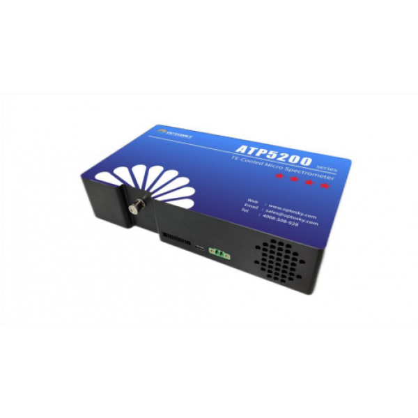
ATP5200 is the fifth generation of TE-cooled high performance spectrometer, which is self-developed by Optosky. It uses a back-thinned TE-cooled linear CCD with a semi-conductor cooling technology. The CCD can set in constant temperature environment (up to -10 degree), which greatly reduces sensor noise at an excellent
signal-to-noise ratio (about 2 times higher than competitors level), and it improves the reliability, so the measurements results can not change with the ambient temperature.
Meanwhile, it uses lowest noise CCD signal processing pcb to reach a noise less than 3 counts, which still the best low noise level.
The ATP5200 can receive SMA905 fiber optic input or free-space light to output spectral data via USB2.0 or UART port. It connects to 5V DC power supply, easy-to-integrate to wide industrial spectroscopy application.
| Detector | |
| Detector type | ATP5200/ATP5200-4: Linear array CCD ATP5200P/ATP5200R: Area array back-thinned CCD |
| Spectral range | 180-1180 nm |
| Effective pixels | ATP5200: 2048 ATP5200-4: 4096 ATP5200P/ATP5200R: 2048×64 |
| Dynamic range | ATP5200/ATP4500-4: 10000: 1 ATP5200P/ATP5200R: 15000: 1 |
| Pixels dimension | ATP5200: 200μm×14μm ATP5200-4: 200μm×7μm ATP5200P/ATP5200R: 14μm×14μm |
| Optical parameter | |
| Focal distance | 98 mm for incidence / 107 mm for output |
| Optical resolution | 0.01-3 nm (Depend on range & slit) |
| Incident Interface | SMA905 connector,free space |
| Signal-to-noise | ATP5200/ATP4500-4: 450:1 ATP5200P/ATP5200R: 15000: 1 |
| Working temperature | -10°c to + 50°c |
| Cooling temperature | -5°c |
| Wavelength range | 180-1180nm |
| Slit Size | 5, 10, 25, 50, 100, 150, 200 μm (optional) |
| Optical Design | F/4 crossed asymmetrical Czerny-Turner |
| Physical parameters | |
| Dimensions | 208×120×47 mm^3 |
| Weight | 1.5-1.7kg |
| Electrical parameter | |
| A/D conversion resolution | ATP5200/ATP4500-4: 16 bit ATP5200P/ATP5200R: 18 bit(Output 16 bit) |
| Integration time | ATP5200/ATP4500-4: 400μs~ 10s ATP5200P/ATP5200R: 5 ms - 30 min |
| Interface | USB 2.0 |
| Supply voltage | DC 5V±10% |
| Operating current | <2.3A |
| Storage temperature | -20°c to + 70 °c |
- Detector: Back-illuminated CCD (cooled to -10 ℃)
- Detector pixels: 2048 pixels
- Special optimization for UV or IR: UV optimization: ATP5200P / Infrared optimization: ATP5200R
- Ultra-low noise CCD signal processing circuit
- Maximum spectral range: 190-1100 nm(maximum width of 900 nm)
- Spectral resolution: 0.1-3 nm
- Optical path structure: cross C-T
- Integration time: 10ms-65s
- Power supply: DC 5V±10% @ <2.3A
- ADC bits depth:18 bit, 570KHz ADC
- 20-pin double-row expansion interface
- Light connector: SMA905 or free space
- Output data port: USB Type-C (High speed) or UART
- Raman spectrometer, online Raman analysis
- Micro volume spectrophotometer
- Weak fluorescent light detection
- Reflectance, Transmittance, Absorbance detection
- Fruit Sorting


