atomic force microscopy
Availability: In Stock
atomic force microscopy
Download Data Sheet
Product Code: ATRA8300-AFM
application
Atomic Force Microscopy (AFM) was developed to overcome a fundamental drawback of scanning tunneling microscope (STM) - it can only image conductive or semiconducting surfaces. The advantage of AFM is that it can image almost any type of surface, including polymers, ceramics, composites, glass, and biological samples.
Unlike scanning tunneling microscopy, Atomic Force Microscopy does not require a conductive sample. Instead of using the quantum mechanical effects of tunneling, atomic forces are used to map the interaction of the tip with the sample.
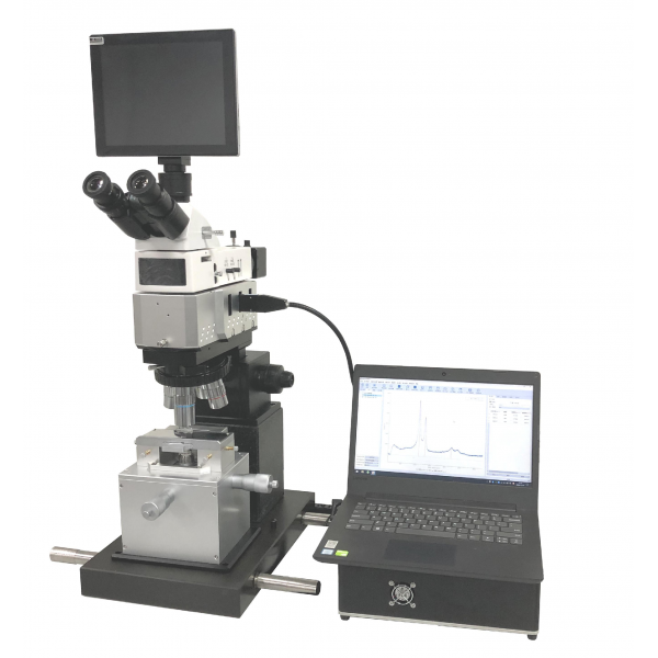
Atomic Force Microscopy is simultaneously equipped with optical two-dimensional measurement and atomic force microscope three-dimensional measurement functions.
| Microscope Module | |
| Operating mode | Contact mode, tap mode |
| Optional mode | Friction/lateral force, amplitude/phase, magnetic/electrostatic force |
| Force spectrum curve | F-Z force curve, RMS-Z curve |
| Objectives | 5X/10X/20X/50X plan apochromatic objective lens |
| XY scan range | 50×50um,20×20um and 100×100um optional |
| Z scan range | 5um,2.5um and 10um optional |
| Scan resolution | Horizontal 0.2nm, vertical 0.05nm |
| Sample size | Φ≤68mm,H≤20mm |
| Optical eyepieces | 10X |
| Optical focus | Coarse and fine manual focusing |
| Monitor | 10.1-inch flat panel display with image measurement function |
| Illumination System | LED Kohler illumination |
| Camera | 5 megapixel CMOS sensor |
| Scan rate | 0.6Hz~30Hz |
| Scan angle | 0~360° |
| Operating environment | Windows XP/7/8/10 operation system |
| Communication interface | USB2.0/3.0 |
Can be combined with a Raman spectrometer to expand functionality.
Precision probe positioning device, laser spot alignment adjustment is very simple.
The laser detection head and sample scanning table are integrated, with a very stable structure and strong anti-interference ability.
Single axis drive sample automatically approaches the probe vertically, making the needle tip to scan perpendicular to the sample .
Intelligent needle feeding method for motor controlled piezoelectric ceramic automatic detection, protecting probes and samples.
Ultra high magnification optical positioning system for precise positioning of probe and sample scanning areas.
Integrated scanner nonlinear correction user editor for nano characterization and measurement accuracy better than 98%.
Polymers
Semiconductors & microelectronics
Material sciences
Biomolecules & membranes
Graphene & 2D materials


