| Detector | |
| Detector type | Hamamatsu s16011 |
| Effective pixels | 2048*64 |
| Detector model | TE-cooled back-illuminated CCD (cooling to -10C) |
| Sensitivity | CCD node sensitivity: 6.5uV/e- |
| Dark noise | CCD Readout Noise:6e- |
| Pixel size | 14μm×14μm |
| Optical parameter | |
| Focal distance | 98 mm for incidence / 107 mm for output |
| Optical resolution | 7-9 cm﹣¹ |
| Dynamic range | 10000:1 |
| Working temperature | -10℃ to +45℃ |
| Working humidity | <90% |
| Trigger | YES/IN and OUT |
| Wavelength range | 150﹣¹ to 4300 ﹣¹ cm-1 |
| SNR | >900:1 |
| Optical Design | Crossed C/T |
| Physical parameters | |
| Size | 217×110×52 mm |
| Weight | 1.6kg |
| Sealing | Anti-sweat |
| Electrical parameter | |
| A/D conversion resolution | 18 bit (Workable Output 16bit) |
| Integration time | 1ms - 30 mins |
| Interface | USB 2.0 or Free space |
| Supply voltage | DC 5V±10% |
| Storage temperature | -20°C to +70°C |
- Back-thinned CCD (cooled down to -10C)
- Customized Raman shift 150 cm﹣¹ to 4300 cm ﹣¹
- Optical resolution: 7-12 cm﹣¹ at slit 25μm (Customized resolution & slit)
- SNR: 900:1
- Dynamic Range: 10000: 1
- Integration time: 1ms to 30 min
- Free Raman spectrometer software
- Configured Raman spectrometer, Raman probe and laser support self setup Raman system
- Raman spectrometer
- Online Raman spectroscopy analysis
- Material identification
- Pharmaceuticals Analysis
- Medical & Life Science
- Energy, Oil & Gas
- Sorting fruits, plastics, polymers
Which are 4 best micro spectrometer applied to Raman spectrometer from Optosky store?
ATP2000P CMOS Cooled 0 degree, the cheapest cost, good performance-to-price rate
ATP5020 Cooled -5 degree, High performance cost less, super high resolution
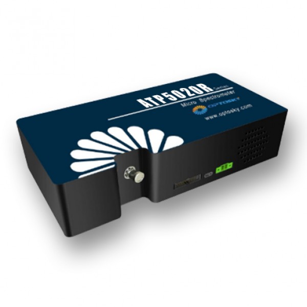
ATP5020R cooled -10 degree,NIR response enhanced, integration time 6ms -30 mins
ATP6500 Cooled -20 degree, Super high SNR & Dynamic range, Integration time 10ms-1.3 hrs
Which detector used for the ATP5020P?
ATP5020P uses Hamamatsu s11850 with uv response enhanced
ATP5020R uses Hamamatsu s11850 with NIR response enhanced
How to choose Optosky TE-cooled spectrometer series?
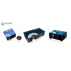
ATP5100 Ultra-miniature, Cooled BT CCD, sized up to a coin.
ATP5040 crossed C-T, TE-cooled 4096 pixels CMOS external cooling, high sensitivity
ATP5020P crossed C-T, Hamamatsu CCD cooled, higher sensitivity, SNR & dynamic range is higher than Maya.
ATP5030P M-shape C-T, higher resolution and low stray light, Hamamatsu CCD
ATP5030 (2048pixels) & ATP5034 (4096pixels) CMOS+TE-cooler, M-shape C-T, high resolution
ATP5330 (2048pixels) & ATP5334 (4096pixels) Thin, cooled CMOS+TE cooled, M-shape C-T, super high resolution
How many types of topology structure of optical path for a spectrometer?
There are commonly divided into 4 types of optical path, including crossed C-T, M-shape C-T, concave grating optical path, transmittance grating opitcal path.
Crossed C-T: ATP2000P,ATP2002, ATP2400, ATP1010, ATP5020P, ATP5040, ATP6500
M-shape C-T: ATP3030, ATP3034, ATP3330/4 ATP5030, ATP5034, ATP5330/4
Concave grating: ATP4230, ATP4020, ATP4050, ATP4070
let's see the M-shape optical path looks like a number "3", so our models uses the 3rd number "3" to indicate M-shape optical path models.
In generally, topology structure can decide resolution, sensitivity, stray light, and size of a spectrometer.
Crossed C-T topology structure employs better sensitivity and compact size.
M-shape C-T employs higher resolution and better stray light.
Concave grating optical path employs high stray light.


