Your shopping cart is empty!
Online Thin-Film Thickness Mapper


SM210 is a film thickness measuring instrument based on the principle of spectrophotometric interference. It uses xenon lamp light source emitted wide wavelength light, part of the workpiece surface and the sensor head internal reflection surface back to the sensor head interior, two reflective beams interfere with each other, the intensity of each wavelength of interference light depends on the spacing between the reflector surface, when the spacing is an integer multiple of the wavelength, it will reach the relative maximum interference with the help of a spectroscope interference light into different wavelengths. The light intensity distribution of the wavelength can be obtained, and the distance between the reflecting surfaces can be calculated after the waveform analysis of the distribution. The maximum mapping range of its thickness can reach 39nm-2.1um.
Availability: In Stock
Online Thin-Film Thickness Mapper
application
SM210 is a film thickness measuring instrument based on the principle of spectrophotometric interference. It uses xenon lamp light source emitted wide wavelength light, part of the workpiece surface and the sensor head internal reflection surface back to the sensor head interior, two reflective beams interfere with each other, the intensity of each wavelength of interference light depends on the spacing between the reflector surface, when the spacing is an integer multiple of the wavelength, it will reach the relative maximum interference with the help of a spectroscope interference light into different wavelengths. The light intensity distribution of the wavelength can be obtained, and the distance between the reflecting surfaces can be calculated after the waveform analysis of the distribution. The maximum mapping range of its thickness can reach 39nm-2.1um.
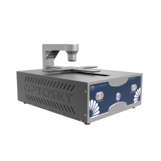
SM210 optical interference multilayer thickness measuring instrument is built by measuring sensor head, controller and upper computer software, combined with the unique algorithm technology of Optosky, to provide users with a new generation of leading multilayer thickness measuring instrument.
| Detector | |
| Power supply | 24V DC |
| Infrared spectroscopy | |
| Linearity | ±0.3μm |
| Optical parameter | |
| Accuracy | ±2nm or 0.2% |
| Monitor probes | |
| Measuring Range | 30nm-100um |
- Using xenon light source, wide band range (190nm-1100nm), high luminous efficiency and long life;
- From single layer to multiple layers, stability measurement can be achieved;
- Adhesion layer can also achieve stable measurement; Wide measurable range 39nm-2.1um;
- The sensor head has no circuit, no electromagnetic interference, no heat;
- Small, light weight, installation space is not limited;
- The selection of "six-wind-one" type 7-core Y-type flexible optical fiber can not only adapt to frequent and high-speed movement on the production line, but also improve the utilization rate of reflected light, thereby improving the signal-to-noise ratio;
- The software interface is intuitive, easy to operate and time-saving; Fast surveying and mapping speed;
Virtually all smooth, translucent or low absorption coefficient films can be mapped, which includes almost all dielectric and semiconductor materials, including silicon dioxide,nitriding layer,diamond-like carbon,polycrystalline silicon, polycrystalline silicon, photoresist, macromolecule, polyimide, amorphous silicon,etc.
Optical glass of Ohara and Schott
Plastic:Acrylic,Acrylate,Lucite,Perspex,Plexiglass,PET,Estar,Melinex,Mylar,Polyacrylate,Polyethylene,PE,Polyethene,Styrene - acrylanitrile,Styrene.
Semiconductor, Compound semiconductor:Aluminum gallium arsenide,Aluminium oxide,Aluminium compounds,CdTe,CoSi2,GaN,GaAs,GaP,GaSb,Indium compounds,Magnesium compounds,Si,Silicon compounds,HfO2,PbS,PbSe,
TiN,TiO2,TiSi2,ZrO2.
Metal target material:Ag,Al,Au,Co,Cr,Cu,Ge,Mo,Nb,Ni,Pt,Rh,Ta,Ti,W
Others:AlCu,Cellulose,KCl,Quartz,Fused Silica,Fused Silica,Silica,Thermal Oxide,ThermalOxide
- Semiconductor coating: photoresist, oxide, desalination layer, silicon-on-insulator, wafer back grinding
- Liquid crystal display: gap thickness, polyimide, ITO transparent conductive film
- Optical coating: hard coating, anti-reflection layer
- Microelectronic system: photoresist, silicon film, printed circuit board
- Biomedical: medical equipment, Parylene